What Is PCBA? A Guide to Printed Circuit Board Assembly
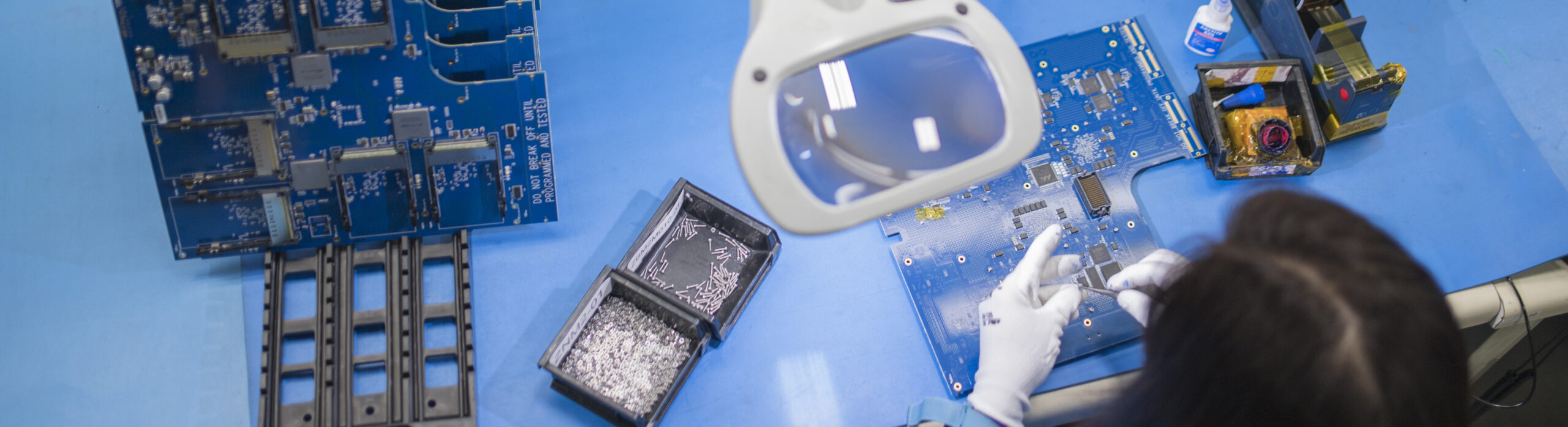
PCBA stands for printed circuit board assembly, the process of mounting and soldering electronic components onto a bare printed circuit board (PCB) to create a functional electronic assembly. PCBA manufacturing covers the production steps required to turn the fabricated board into an assembled product that can be inspected, tested and integrated into a larger system.
Understanding the difference between PCB and PCBA is important when sourcing electronics manufacturing because the two refer to different stages of production.

PCB vs. PCBA: What Is the Difference?
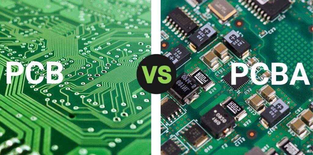
A PCB is the bare board that provides the mechanical structure and electrical connections for an electronic design. It contains conductive copper traces, pads, vias, insulating layers and other features defined by the design, but it does not yet contain the electronic components required for the product to operate.
A PCBA is the assembled board after components such as integrated circuits, resistors, capacitors and connectors have been installed and soldered. Depending on the product, a completed PCBA may then undergo electrical or functional testing before moving into box-build or system-level integration.
How Does the PCBA Manufacturing Process Work?
The exact PCBA manufacturing process depends on board complexity, component technology, production volume and product requirements. However, most assemblies move through several core processes.
For surface mount technology (SMT), solder paste is first deposited onto designated PCB pads using a stencil. Solder paste inspection (SPI) can measure the deposited paste before component placement, allowing process issues to be identified early.
Automated placement equipment then positions surface-mount components onto the board. Modern assemblies can include very small packages, fine-pitch devices and components such as BGAs, where solder connections sit underneath the package rather than around its perimeter.
The populated board passes through a controlled reflow oven, where the solder paste melts and forms permanent electrical and mechanical connections. Products that contain through-hole components may require additional processes such as wave soldering, selective soldering or manual assembly.
Many PCBAs combine surface-mount and through-hole components, and components may be populated on one or both sides of the board. In these cases, the manufacturing sequence is planned around the component mix, soldering processes and thermal requirements of the assembly.
Inspection and Testing in PCBA Manufacturing
Inspection throughout production helps identify defects before they move further downstream. Automated optical inspection (AOI), for example, can check component placement and visible solder joints, while X-ray inspection provides visibility into connections that optical systems cannot see directly, including solder joints underneath BGA packages.
The inspection and test strategy depends on the product and its requirements. A PCBA may use a combination of:
- Solder paste inspection (SPI)
- Automated optical inspection (AOI)
- X-ray inspection
- Electrical and functional testing
Industry standards also define requirements and acceptance criteria for electronic assemblies. IPC-A-610 addresses the acceptability of electronic assemblies, while J-STD-001 establishes requirements for soldered electrical and electronic assemblies.
For complex products, process control extends beyond final inspection. Traceability systems can connect materials, components and production data to individual assemblies, helping manufacturers investigate defects, manage quality records and maintain visibility throughout production.
Post-Assembly Processing and Conformal Coating
Depending on the product and operating environment, a PCBA may require additional processing after soldering, inspection and testing. These steps prepare the assembly for its intended application and can provide additional protection against environmental exposure.
Conformal coating is one common example. A thin protective coating is applied over selected areas of the assembled board to help protect circuitry from moisture, dust, contamination and other environmental conditions. The coating material, application method and required coverage depend on the product specification and operating environment.
Other post-assembly requirements may include cleaning, masking, labeling or additional mechanical operations. These processes need to be defined as part of the manufacturing documentation so they can be applied consistently from one production build to the next.
From PCBA to a Finished Electronic Product
Printed circuit board assembly is often one stage within a larger electronics manufacturing program. After assembly and testing, PCBAs may require conformal coating, mechanical assembly, cable and harness installation, enclosure integration or system-level testing.
At Dynamic Source Manufacturing, PCBA manufacturing supports both new product introduction and ongoing production at our facilities in Calgary, Alberta and Tempe, Arizona. Our capabilities include SMT and through-hole assembly, fine-pitch and 01005 component placement, SPI, AOI and X-ray inspection, wave and selective soldering, conformal coating, functional testing and Level 4 material traceability.
For OEMs moving a product from prototype into production, the manufacturing process should also account for design manufacturability, test strategy, component availability and future production requirements early in the program. Addressing these factors before volume increases can reduce avoidable production issues and support a more controlled transition into ongoing manufacturing.
To discuss a PCBA program or upcoming build, contact DSM’s team or request a quote.
Reach out to DSM today: dsmsales@dynamicsourcemfg.com
Book a facility tour: Contact DSM